ここから本文です。
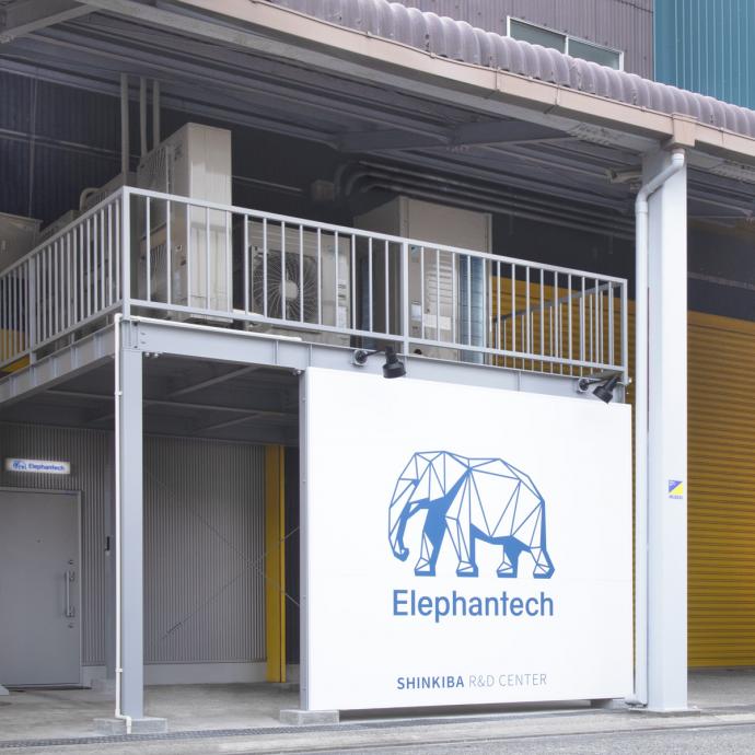
エレファンテック株式会社(企業紹介)Elephantech Inc.
知恵の経営、元気印、経営革新、チャレンジ・バイの各認定等を受けた中小企業を紹介するページです。

金属インクジェット印刷によるプリント基板でパラダイムシフトを Paradigm shift with printed circuit boards using metal inkjet printing
「ZET-summit 2024」で「Global Deeptech賞」を受賞されたエレファンテック株式会社(外部リンク)(東京都)を訪問。伊藤CFOにお話をおうかがいしました。
インク・印刷機開発、印刷、めっきまで社内一貫対応 In-house integrated support from ink and printing machine development to printing and plating
--御社のように、インクジェット印刷でプリント基板を作るという方法は、どのようにして発想されたのでしょうか?How did you come up with the idea of using inkjet printing to make printed circuit boards like your company does?
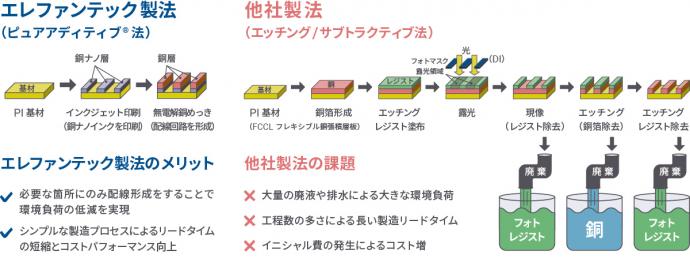
伊藤)この手法自体は、当社が思いついたというより、この業界では誰もが考えたことがあろう手法です。現在主流となっているエッチング/サブトラクティブ法は、1940年代には確立された方法ですが、不要なものを取り除いていくわけですから、皆がもったいないなと思っていたわけです。そのような中で、大手企業などが、代わる手法としてインクジェット方式の研究開発に取り組んできたわけですが、技術的に簡単ではなくうまくいかなかったわけです。This method itself is not one that our company came up with, but rather one that everyone in this industry has thought of. The etching/subtractive method that is now mainstream was established in the 1940s, but since it removes unnecessary things, everyone thought it was a waste. Under such circumstances, major companies and others have been working on research and development of inkjet methods as an alternative method, but it was not technically easy and did not work out.
--それなのに御社はどうしてうまくいったのですか?How did your company succeed?
伊藤)当社では、インクの開発から印刷装置の開発まで一貫対応しているのです。通常は、別々の会社で行われるこれらのことを自社内で行っているので、すり合わせがしやすいのです。Our company provides integrated support from ink development to printing equipment development. These things that are normally done by separate companies are done in-house, which makes it easy to coordinate.
--むちゃむちゃ「ものづくり」の会社さんなのですね!もう1つ質問なのですが「無電解銅めっきで金属を成長させていく」とは?It's a manufacturing company! I have another question: What does it mean to "grow metal using electroless copper plating"?
伊藤)当社では、通常のプリント基板(PCB)の代替を目指しています。印刷で形成される配線は、通常の紙への印刷等と同様の仕組みですので、厚みが1μmもありません。これでは、PCBに求められる電流量を実現出来ませんので、印刷配線をめっきシード層としてめっき処理を施すことで、必要な配線厚みまで金属を成長させているのです。At our company, we aim to replace ordinary printed circuit boards (PCBs).The wiring formed by printing uses the same mechanism as printing on ordinary paper, so it is less than 1 μm thick. Since the required amount of current cannot be achieved, the metal is grown to the required wiring thickness by plating using the printed wiring as a plating seed layer.
--まさかそれも社内で?Is that even within the company?
伊藤)はい。材料開発、インクジェット印刷、無電解銅めっきまで一貫対応しています。Yes. We provide comprehensive support from material development, inkjet printing, and electroless copper plating.
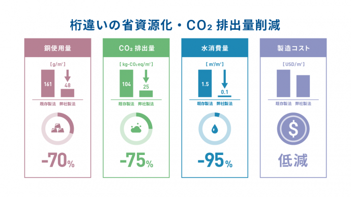
桁違いの省資源化・CO2排出量削減 Significant resource savings and CO2 emissions reduction
--素晴らしいですね。しかも省資源化やCO2排出量削減にも寄与されるものなのですよね。It is wonderful. Moreover, it also contributes to resource conservation and CO2 emissions reduction.
伊藤)はい。当社製法では、銅箔から削っていって配線を形成するのに代わり、必要な部分にのみ印刷を行っております。結果として、従来型製法で削りとられ捨てられてしまう銅は実際に利用される銅の2倍以上であることから、銅使用量を大幅に削減、CO2排出量も約4分の1とすることができます。また、従来型製法にて削り取られる銅は、酸化銅液として廃液になってしまいます。この廃液排出が発生しないことも環境面で大きなインパクトがあると認識しております。Yes. With our manufacturing method, instead of cutting away from copper foil to form wiring, we print only on the necessary areas.As a result, the copper that would be scraped off and thrown away with conventional manufacturing methods is actually used. The amount of copper used in this process is more than twice that of the copper used in the production process, so it is possible to significantly reduce the amount of copper used and reduce CO2 emissions to about one-fourth.In addition, the copper that is scraped off using conventional manufacturing methods is replaced by copper oxide. The liquid becomes waste liquid.We recognize that not discharging this waste liquid has a large impact on the environment.
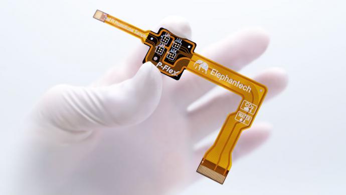
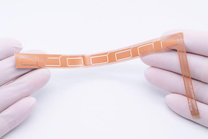
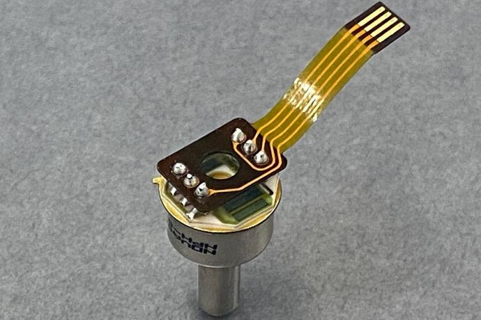
湾曲や圧力に対応できる「フレキシブル基板」 "Flexible substrate" that can handle bending and pressure
--用途としてはどういった分野のものが多いのですか?In what fields are they most often used?
伊藤)スマートフォンや家電、自動車、産業機器など、ほとんど全ての電子機器に利用されています。フレキシブル基板は、一般にプリント基板と聞いてイメージされるPCのマザーボードのような板状のものではなく、薄く折り曲げ可能で柔軟性に優れたものですが、製品設計の自由度を高めることから幅広く利用されているのです。具体的な利用目的としては、公表している当社製品の採用事例となりますが、湾曲形状のスイッチ部分や、圧力センサーモジュールなどとなります。They are used in almost all electronic devices such as smartphones, home appliances, automobiles, and industrial equipment.Flexible circuit boards are not plate-shaped like PC motherboards, which is what you think of when you think of printed circuit boards, but are thin and bendable. Although it has excellent flexibility, it is widely used because it increases the degree of freedom in product design.As for the specific purpose of use, this is an example of the use of our products that has been published, but curved shapes switch parts, pressure sensor modules, etc.
プリント基板業界を支える Supporting the printed circuit board industry
--最初からこういう分野を狙ってやってこられたのですか?Did you aim for this field from the beginning?
伊藤)いえ、最初は研究用、試作用の受託生産でスタートしたのです。しかし、事業として成立させるためには「量」を担保する必要があるということで量産化にこぎつけたわけです。Although we have been aiming for this field from the beginning, we started with contract manufacturing for research and prototyping purposes. However, in order to succeed as a business, it was necessary to guarantee "quantity", so we reached mass production.
--そうだったのですね。現在、特に注力されている領域などありますか?That's right. Are there any areas in particular that you are currently focusing on?
伊藤)コンピュータ周辺機器、カメラ、ゲーミング機器、EV向け電池制御システムなどですね。These include computer peripherals, cameras, gaming equipment, and battery control systems for EVs.
--なるほど。I see.
伊藤)プリント基板の生産は薄利多売です。だから、同業企業やあるいは周辺企業の事業承継や、国内での生産基盤の拡大を行い、業界を支えていこうと思っています。Printed circuit board production is low profit and high sales. Therefore, we are planning to support the industry by taking over the business of similar or peripheral companies and expanding our domestic production base.
--素晴らしいですね!
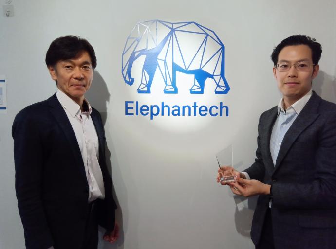
ZET-summitに登壇された松浦部長 (左)とインタビューを受けてくださった伊藤CFO
お問い合わせ